- 您现在的位置:买卖IC网 > Sheet目录368 > W25Q64FVSFIG (Winbond Electronics)IC SPI FLASH 64MBIT 16SOIC
W25Q64FV
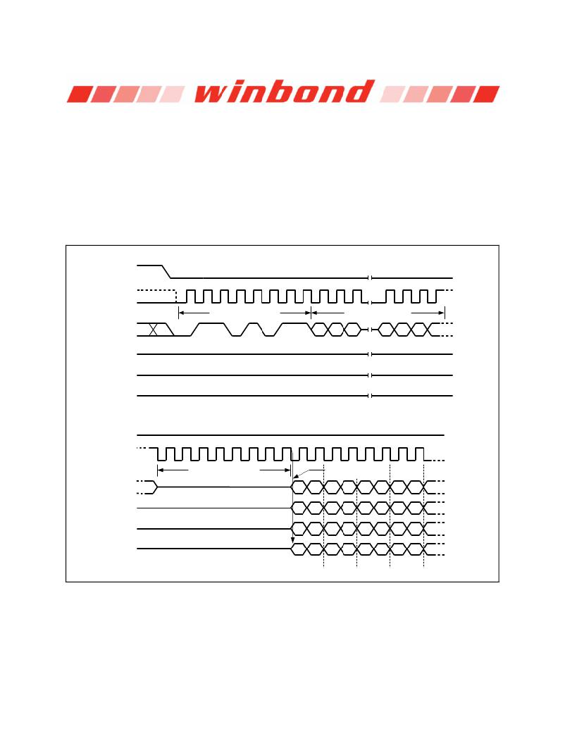
6.2.14
Fast Read Quad Output (6Bh)
The Fast Read Quad Output (6Bh) instruction is similar to the Fast Read Dual Output (3Bh) instruction
except that data is output on four pins, IO 0 , IO 1 , IO 2 , and IO 3 . A Quad enable of Status Register-2 must be
executed before the device will accept the Fast Read Quad Output Instruction (Status Register bit QE
must equal 1). The Fast Read Quad Output Instruction allows data to be transferred from the W25Q64FV
at four times the rate of standard SPI devices.
The Fast Read Quad Output instruction can operate at the highest possible frequency of F R (see AC
Electrical Characteristics). This is accomplished by adding eight “dummy” clocks after the 24 -bit address
as shown in Figure 13. The dummy clocks allow the device's internal circuits additional time for setting up
the initial address. The input data during the dummy clocks is “don’t care”. However, the IO pins should
be high-impedance prior to the falling edge of the first data out clock.
/CS
Mode 3
0
1
2
3
4
5
6
7
8
9
10
28
29
30
31
CLK
Mode 0
Instruction (6Bh)
24-Bit Address
IO 0
23
22
21
3
2
1
0
IO 1
IO 2
IO 3
/CS
* = MSB
High Impedance
High Impedance
High Impedance
*
31
32
33
34
35
36
37
38
39
40
41
42
43
44
45
46
47
CLK
Dummy Clocks
IO 0 switches from
Input to Output
IO 0
IO 1
IO 2
IO 3
0
High Impedance
High Impedance
High Impedance
4
5
6
7
0
1
2
3
4
5
6
7
0
1
2
3
4
5
6
7
0
1
2
3
4
5
6
7
0
1
2
3
4
5
6
7
Byte 1
Byte 2
Byte 3
Byte 4
Figure 13. Fast Read Quad Output Instruction (SPI Mode only)
- 33 -
Publication Release Date:
October 07, 2013
Revision L
发布紧急采购,3分钟左右您将得到回复。
相关PDF资料
W25Q80BVSNIG
IC SPI FLASH 8MBIT 8SOIC
W25Q80BWSSIG
IC FLASH SPI 8MBIT 8SOIC
W25X40BVZPIG
IC SPI FLASH 4MBIT 8WSON
W25X64VZEIG
IC FLASH 64MBIT 75MHZ 8WSON
W25X80AVDAIZ
IC FLASH 16MBIT 100MHZ 8DIP
W29GL032CB7A
IC FLASH 32MBIT 70NS 48TFBGA
W29GL064CB7S
IC FLASH 64MBIT 70NS 48TSOP
W29GL128CL9T
IC FLASH 128MBIT 90NS 56TSOP
相关代理商/技术参数
W25Q64FVSFIG TR
制造商:Winbond Electronics Corp 功能描述: 制造商:Winbond Electronics Corp 功能描述:IC FLASH 64MBIT 104MHZ 16SOIC
W25Q64FVSFIP
制造商:WINBOND 制造商全称:Winbond 功能描述:3V 64M-BIT SERIAL FLASH MEMORY WITH DUAL/QUAD SPI & QPI
W25Q64FVSSIG
功能描述:IC SPI FLASH 64MBIT 8SOIC RoHS:是 类别:集成电路 (IC) >> 存储器 系列:SpiFlash® 标准包装:2,500 系列:- 格式 - 存储器:EEPROMs - 串行 存储器类型:EEPROM 存储容量:1K (128 x 8) 速度:100kHz 接口:UNI/O?(单线) 电源电压:1.8 V ~ 5.5 V 工作温度:-40°C ~ 85°C 封装/外壳:8-TSSOP,8-MSOP(0.118",3.00mm 宽) 供应商设备封装:8-MSOP 包装:带卷 (TR)
W25Q64FVSSIG TR
制造商:Winbond Electronics Corp 功能描述:SPIFLASH, 64M-BIT, 4KB UNIFORM 制造商:Winbond Electronics Corp 功能描述:IC FLASH 64MBIT 104MHZ 8SOIC 制造商:Winbond 功能描述:SPIFLASH, 64M-BIT, 4KB UNIFORM
W25Q64FVSSIG/TRAY
制造商:Winbond Electronics Corp 功能描述:
W25Q64FVSSIP
制造商:WINBOND 制造商全称:Winbond 功能描述:3V 64M-BIT SERIAL FLASH MEMORY WITH DUAL/QUAD SPI & QPI
W25Q64FVTCIG
制造商:Winbond Electronics Corp 功能描述:64MBIT SPI
W25Q64FVTCIP
制造商:WINBOND 制造商全称:Winbond 功能描述:3V 64M-BIT SERIAL FLASH MEMORY WITH DUAL/QUAD SPI & QPI
